Atmel "AVR" Architecture - Part I
An intermediate guide for Low-level concepts of AVR Microcontroller
(Basics of AVR architecture & program execution process)
(Basics of AVR architecture & program execution process)


Welcome Note :
Welcome to the Low level guide for AVR MCUs (Micro Controller Unit). This tutorial is targeted towards people having basic knowledge of MCUs and Embedded C programming. If not, please refer to any good AVR beginners tutorial on the internet and I'm sure that there are plenty of 'em. Throughout the entire tutorial I will be using Atmega32A MCU for showing examples codes (Probably not in this tutorial). In this tutorial I'll be talking about the architecture of AVR MCUs specifically Atmega32A. But, believe me, the concepts and architecture are pretty similar in all MCUs. What is different is the resources and features of the particular MCU. So, let's get started.
Prerequisites :
Basics of AVR:
AVR MCUs are extremely popular MCUs used in various application specially in project prototyping and embedded devices. AVR is a 8-bit RISC architecture (Reduced Instruction Set Computing) microcontroller in market since 1996 which is having on-chip programmable flash memory, SRAM, IO data space & EEPROM. AVR is the first MCU in market which has on-chip flash storage. For more info about the features of any AVR MCU, refer to the datasheet freely distributed by the manufacturer. For this tutorial I'm going to use Atmega32A, so it would be better if you download the corresponding datasheet.
According to the datasheet, the block diagram of its architecture is this (look below) :
Welcome to the Low level guide for AVR MCUs (Micro Controller Unit). This tutorial is targeted towards people having basic knowledge of MCUs and Embedded C programming. If not, please refer to any good AVR beginners tutorial on the internet and I'm sure that there are plenty of 'em. Throughout the entire tutorial I will be using Atmega32A MCU for showing examples codes (Probably not in this tutorial). In this tutorial I'll be talking about the architecture of AVR MCUs specifically Atmega32A. But, believe me, the concepts and architecture are pretty similar in all MCUs. What is different is the resources and features of the particular MCU. So, let's get started.
Prerequisites :
- Basics of Microcontrollers (Very basic, you should know at least what they are)
- Embedded C (Actually it the standard C language with a library built on top of it)
- Atmel Studio (According to me, the best IDE for embedded development) [not needed right now]
- Basic knowledge of Digital Electronics
Basics of AVR:
AVR MCUs are extremely popular MCUs used in various application specially in project prototyping and embedded devices. AVR is a 8-bit RISC architecture (Reduced Instruction Set Computing) microcontroller in market since 1996 which is having on-chip programmable flash memory, SRAM, IO data space & EEPROM. AVR is the first MCU in market which has on-chip flash storage. For more info about the features of any AVR MCU, refer to the datasheet freely distributed by the manufacturer. For this tutorial I'm going to use Atmega32A, so it would be better if you download the corresponding datasheet.
According to the datasheet, the block diagram of its architecture is this (look below) :
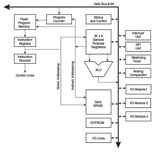
Don't worry if it made no sense to you .. Let's continue with the discussion.
Let's discuss briefly the elements inside this wired looking diagram. Although, having a good knowledge in digital electronics, this is not at all needed.
Data BUS 8 bit : Its an 8-bit parallel data lines by which the data travels inside the MCU (NOTE: this is the reason why AVR is an 8-bit MCU).
ALU: Arithmetic Logic Unit, the core/heart of the entire system where typically all commands get executed.
Data SRAM: It basically pretty similar to the RAM (Random access memory) we see inside our computers.
EEPROM: (Electrically Erasable Programmable Read Only Memory) its very similar to another component in our computer namely HardDisk, i.e. a permanent storage.
I/O lines: These are the bunch of registers which is used as a switches or controls for different features of AVR.
32X8 GPR (General Purpose Registers): This are 32 registers each having 8-bit which is a general storage space for data. But, remember, SRAM is also a temporary storage but these registers have some specialty among all.
Status & Control : A couple of registers which are very special to the MCU & to us also.
Program Counter: This is a register which has a responsibility to track the position of the program that is currently executing.
Flash Memory: It is also a permanent storage but its only for storing the program we write to it.
Instruction Register & Decoder: These are import for the MCU but not too much to us.
The rest of the blocks are different modules for application programming purpose. We'll not discuss them (right now).
Flash memory:
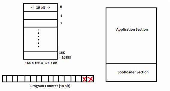
The last digits of the name of the MCU (32 in case of Atmega32A) signifies the amount of flash memory it contains (in KBytes). So, Atmega32A has 32 KB flash memory (more than enough for a standard application program).
This memory is organised in a different manner. As it can be seen from the image below that the 32K X 8B (32768 Bytes) flash is organised in 16K X 16B (32768 Bytes). So the flash memory is having 16 bits (2 bytes) as the smallest unit, which can be addressed via 0 through 16383. In this context, I would like to introduce you to the Program Counter also. Because of the highest address of the flash memory is 16383 (11111111111111 in binary), a PC (which stores address of the currently executing location of the flash) of 14 bits is sufficient. To be a bit more clear, an address 'X' of the flash memory denotes 2 bytes of data, where 'X' ranges from 0 to 16383 (Remember, these numbers are often written in HEX format, i.e. 0x3FFF/ $3FFF. A dollar sign in front of the HEX number is a convention followed by Atmel assembler to denote memory address while coding in low level assembly language).
Btw, the entire flash memory is logically divided into 2 sections namely "Bootloader" section & "Application" section. (More on these later).
Let's discuss briefly the elements inside this wired looking diagram. Although, having a good knowledge in digital electronics, this is not at all needed.
Data BUS 8 bit : Its an 8-bit parallel data lines by which the data travels inside the MCU (NOTE: this is the reason why AVR is an 8-bit MCU).
ALU: Arithmetic Logic Unit, the core/heart of the entire system where typically all commands get executed.
Data SRAM: It basically pretty similar to the RAM (Random access memory) we see inside our computers.
EEPROM: (Electrically Erasable Programmable Read Only Memory) its very similar to another component in our computer namely HardDisk, i.e. a permanent storage.
I/O lines: These are the bunch of registers which is used as a switches or controls for different features of AVR.
32X8 GPR (General Purpose Registers): This are 32 registers each having 8-bit which is a general storage space for data. But, remember, SRAM is also a temporary storage but these registers have some specialty among all.
Status & Control : A couple of registers which are very special to the MCU & to us also.
Program Counter: This is a register which has a responsibility to track the position of the program that is currently executing.
Flash Memory: It is also a permanent storage but its only for storing the program we write to it.
Instruction Register & Decoder: These are import for the MCU but not too much to us.
The rest of the blocks are different modules for application programming purpose. We'll not discuss them (right now).
Flash memory:
The last digits of the name of the MCU (32 in case of Atmega32A) signifies the amount of flash memory it contains (in KBytes). So, Atmega32A has 32 KB flash memory (more than enough for a standard application program).
This memory is organised in a different manner. As it can be seen from the image below that the 32K X 8B (32768 Bytes) flash is organised in 16K X 16B (32768 Bytes). So the flash memory is having 16 bits (2 bytes) as the smallest unit, which can be addressed via 0 through 16383. In this context, I would like to introduce you to the Program Counter also. Because of the highest address of the flash memory is 16383 (11111111111111 in binary), a PC (which stores address of the currently executing location of the flash) of 14 bits is sufficient. To be a bit more clear, an address 'X' of the flash memory denotes 2 bytes of data, where 'X' ranges from 0 to 16383 (Remember, these numbers are often written in HEX format, i.e. 0x3FFF/ $3FFF. A dollar sign in front of the HEX number is a convention followed by Atmel assembler to denote memory address while coding in low level assembly language).
Btw, the entire flash memory is logically divided into 2 sections namely "Bootloader" section & "Application" section. (More on these later).
GPRs, I/O Space & SRAM memory space:
These memories are organized in another manner than the flash. These memories are different in nature but having a continuous space (logically) inside the MCU. Let's look at the diagram first.
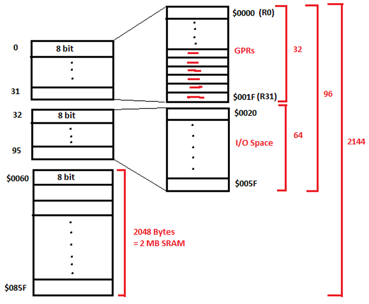
GPRs (General Purpose Registers) are 32 in number each of them being an 8-bit storage, take address from $0000 upto $001F ( Remember the dollar sign !! ya, right, memory addresses. Its not necessary to specify the dollar sign while explaining them in a theoritical manner but I do this for convenience). These are general purpose storage for data. We often use these registers for storing variables and other data while programming the MCU. These registers have special names as R0 upto R31 (Look at the diagram above for more clarification). Now one thing to mention that the last 6 register in this series of registers (R26 upto R31) have special names XL, XH, YL, YH, ZL & ZH (They are pointed in the diagram by red dashes) & also special purposes. So, as an example, $001E is nothing but R30 which is the 31st GPR.
I/O Space is a collection of 64 registers each register having totally different names according to their purposes (We will get into them later), e.g. DDRA, PINB, EEAR, etc. Those who already know embedded C programming, may recognize these names. Apart from their names, they have their usual memory addresses from $20 through $5F (Remember, the GPR memory space continues here). One thing to note that these registers are called usually by their names not by their addresses.
SRAM is a volatile memory of temporary storage which is actually the main "Memory" of an MCU. In the diagram as well as in discussion, I have considered Atmega32A which has 2KB of SRAM, which means 2048 cells of 8-bit each, address ranging from $60 upto $85F (Look !! same thing as before, the address space still continues). These SRAM locations usually accessed via their memory addresses as they don't have special names (Imagine if you have 2048 registers all having different names !! Phewwww...).
Some special Registers are Status Register (SREG), Program Counter (PC). Status register refers to that special register of MCU which keeps track of of the status of the MCU as well as the last arithmetic operation completed on ALU.
The PC is a pointer to the memory address (flash memory) of the next command that will be executed. As I've shown before, PC is a 14 bit register to hold any address ranging from $0000 to $3FFF (The last address of flash memory).
Program Execution & Clock:
As you probably know, a program always coverts down to assembly/ machine code which is nothing but a bunch of binary numbers, regardless of what programming language you use. So, the machine code gets uploaded to the flash memory of the MCU in a particular location (not necessarily at $0000, depends on some settings I'll talk about later). After that, the PC is set to the starting address of the program & its starts executing. The PC is increased by 1 after completion of the previous command (Actually the amount of increment depends of the command also, but for now, forget about this).
Another very important component inside the MCU is a pulse generator or a "Clock" which simply generates square pulses in a constant frequency. The purpose of the Clock is to create a rhythm inside the MCU so that it can make sure about the concurrent processing of each & every module.
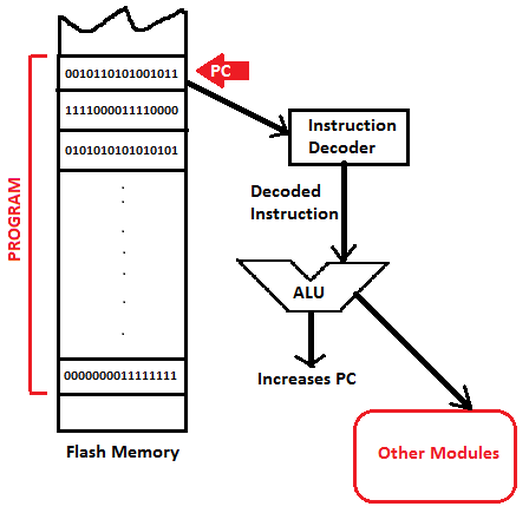
During a single clock pulse, the following things happen:
Step 1. Fetches the command/Instruction at the address of the flash memory pointed by PC.
Step 2. The binary machine code then gets decoded by a "Instruction Decoder".
Step 3. After figuring out the command/Instruction, the ALU starts performing the operation corresponding to the machine code. (Different machine codes correspond to different tasks)
Step 4. The ALU increases the PC by 1 (it actually depends on the instruction, but for now, simplest case can be considered).
Step 5. Goto Step 1.
The above cycle continues till the MCU is properly powered.
This concludes the AVR architecture and the program execution process. In the upcoming part II of this tutorial, I'll cover the Program uploading process, the Interrupts & basics of Bootloader.
Stay tuned ...
